PCIe AHCI Device Driver Development
Implementing High-Performance Storage Interface for Hybrid HDD Systems
By Myung Guk Lee in Technical Projects
August 30, 2022
Project Overview
Led the development of a PCIe AHCI device driver for a Solid State Hybrid Drive (SSHD) system. This innovative storage solution combines HDD capacity with SSD performance by utilizing a PCIe-connected SSD cache for frequently accessed data.
Technical Architecture
System Overview
The SSHD architecture integrates traditional HDD storage with a PCIe-connected SSD cache:
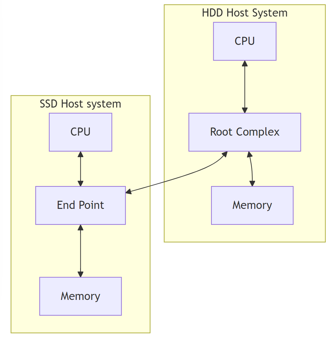 Figure 1: High-level architecture of the Hybrid Storage System
PCIe Port Initialization Flow
The PCIe controller initialization follows a precise sequence to ensure reliable operation:
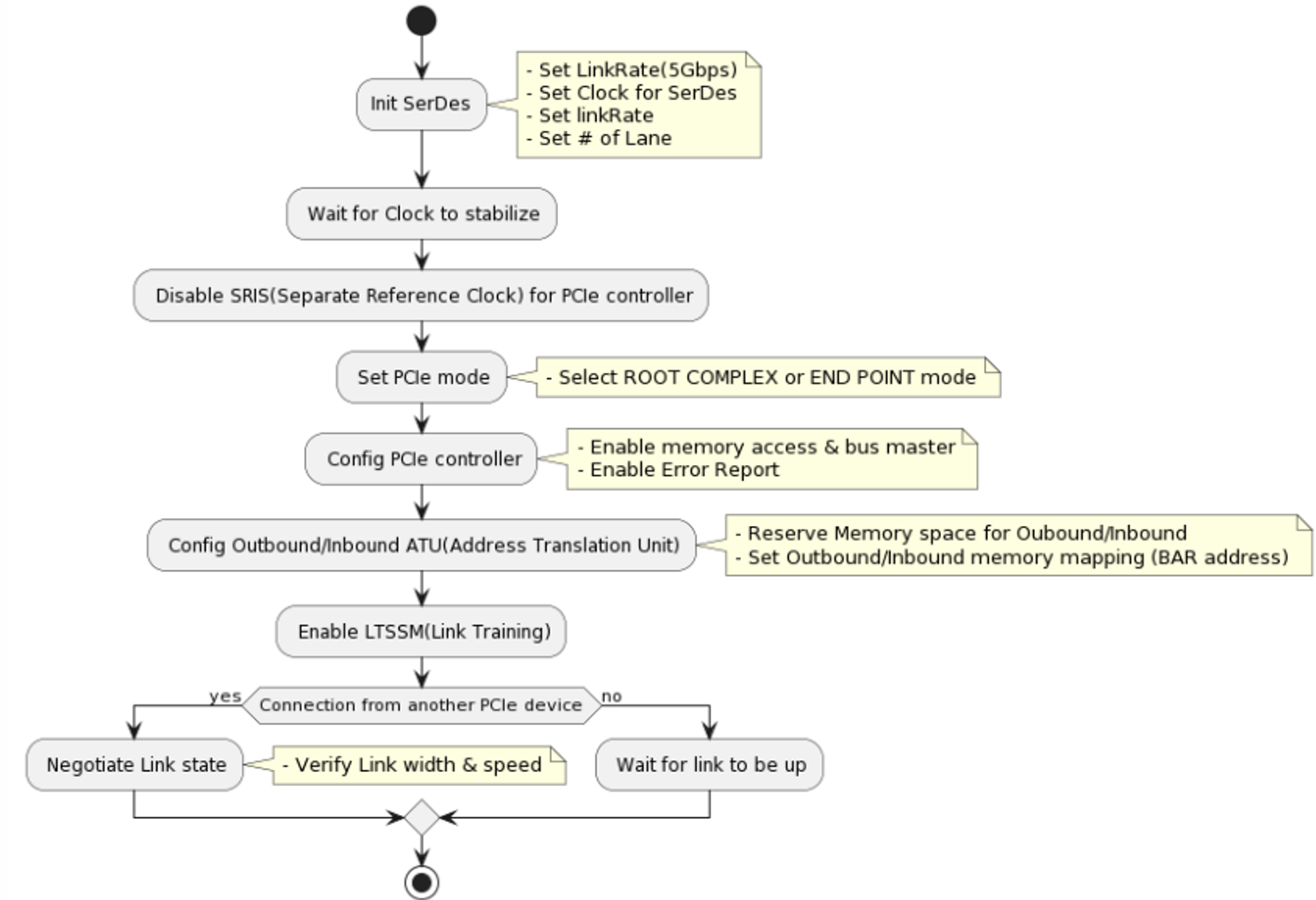 Figure 2: Detailed PCIe port initialization sequence
Implementation Details
Driver Architecture
The PCIe AHCI driver implementation was structured around three key components:
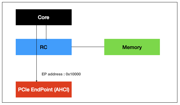
Figure 3: PCIe AHCI Driver Architecture
Memory Mapping Strategy
Implemented efficient BAR (Base Address Register) mapping for optimal performance:
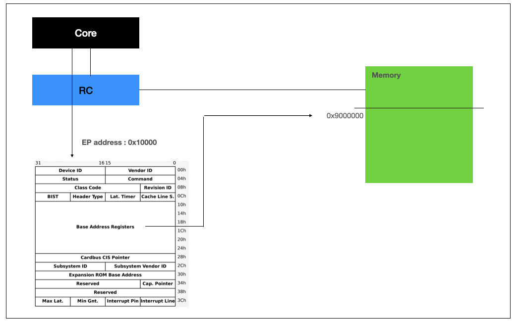 Figure 4: Base Address Register mapping architecture
Key Implementation Steps
- PCIe Configuration Space Management
Configuration Space Layout
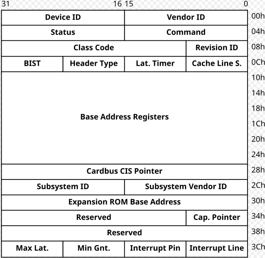 Figure: PCIe Configuration Space Structure
Key Configuration Registers
| Register | Offset | Purpose | Access Type |
|---|---|---|---|
| Vendor/Device ID | 0x00-0x03 | Device identification | Read-only |
| Command | 0x04-0x05 | Device control | Read/Write |
| Status | 0x06-0x07 | Device status | Read-only |
| BAR[0-5] | 0x10-0x24 | Memory/IO space mapping | Read/Write |
| Interrupt | 0x3C-0x3F | Interrupt configuration | Read/Write |
-
AHCI Port Configuration
- Port register initialization
- Command list and FIS base address setup
- Interrupt handling implementation
- Device presence verification
-
DMA Engine Setup
- Command list structure initialization
- PRD (Physical Region Descriptor) table configuration
- Memory-mapped I/O optimization
Protocol Analysis
Link Training and State Management (LTSSM)
The PCIe link establishment process involves multiple states:
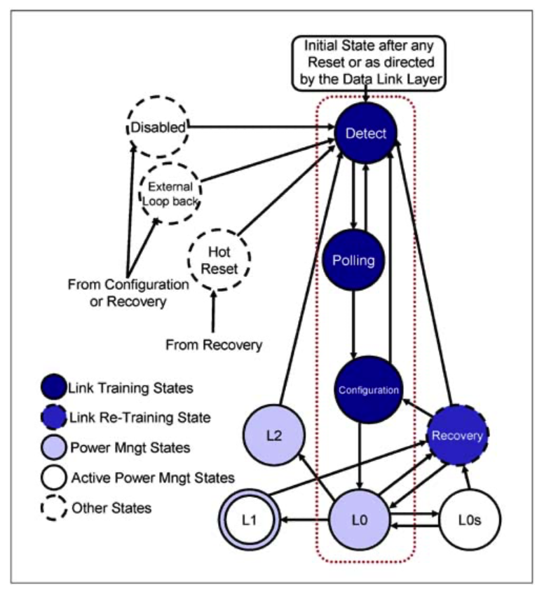 Figure 5: Link Training and State Management flow
| State | Description | Key Operations |
|---|---|---|
| Detection | Initial device presence detection | Electrical idle detection |
| Polling | Training sequence exchange | Symbol lock establishment |
| Configuration | Link width/speed negotiation | Capability exchange |
| L0 | Normal operation state | Active data transfer |
| Recovery | Link retraining/power state transition | Link maintenance |
Packet Transfer Protocol
Data transmission utilizes Transaction Layer Packets (TLP) and Data Link Layer Packets (DLLP):
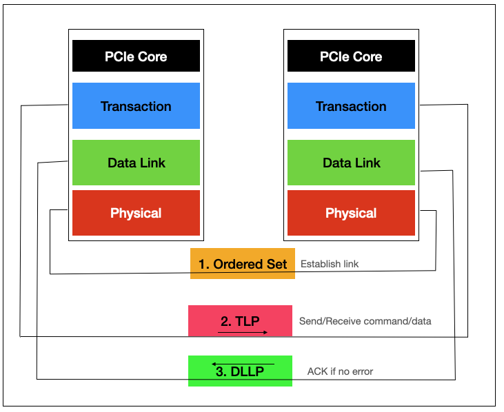 Figure 6: PCIe packet transfer protocol
Performance Optimization
Key Metrics
- Reduced latency through optimized interrupt handling
- Improved throughput with efficient DMA transfers
- Enhanced reliability through robust error handling
Benchmark Results
[Consider adding performance graphs/charts here]
Technical Challenges and Solutions
-
Interrupt Handling
- Challenge: Legacy interrupt limitations
- Solution: Implemented custom interrupt coalescing
-
DMA Performance
- Challenge: Memory alignment issues
- Solution: Implemented aligned buffer management
-
Error Recovery
- Challenge: Link state recovery
- Solution: Developed robust recovery mechanisms
Conclusion
This project successfully delivered a high-performance PCIe AHCI device driver, enabling efficient operation of hybrid storage systems. The implementation provides a foundation for future storage system optimizations.
- Posted on:
- August 30, 2022
- Length:
- 2 minute read, 392 words
- Categories:
- Technical Projects
- Series:
- Device Driver Development